The J-11 (code name Jaws, which the design team never used) was DEC's fourth and last PDP-11 microprocessor design, and the first to be done in CMOS. The project was co-developed with Harris Semiconductor. Bob Supnik was the project leader through 1981, then Dan Casaletto. Paul Rubinfeld was lead engineer on the Data chip, Gil Wolrich on the Control chip and the FPA. Keith Henry wrote the microcode. Circuit design and layout were done by Harris Semiconductor.
The J-11 was intended to put a "capstone" on the PDP-11 family by providing the full functionality and performance of the PDP-11/70 in a microprocessor. Accordingly, the J-11 incorporated most of the architectural ornamentation from the 11/70 -- dual register sets, data space, supervisor mode -- as well as more modern inventions such as SMP support. Microcode-based floating point was standard, with accelerated floating point available as an option. CIS microcode was also intended to be an option.
The J-11 was a chip set consisting of three designs, one of which could be replicated: the Control chip (up to three supported), the Data chip, and the optional FPA chip. The Control and Data chips were implemented in Harris double-poly 4u P-well CMOS. The FPA was implemented in DEC's double-metal 3u NMOS process (ZMOS). Bin points of 3.75Mhz and 4.5Mhz were supported
| Name | Number | Size | Transistors | Comments |
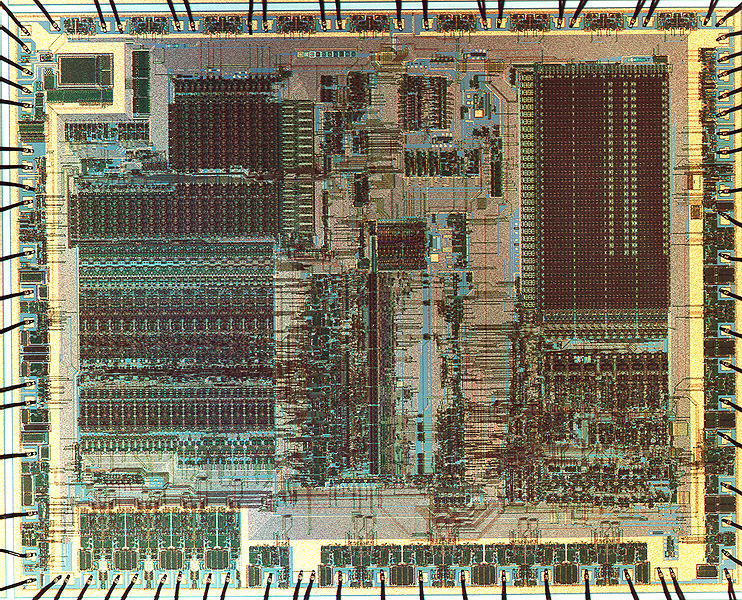
| Data | DC334 | 334x280 | 40,000 | The Data chip implements the instruction execution and memory management
data paths of the J-11 chip set. It shares with the Control chip responsibility
for the external interface and for instruction prefetching. The data chip
operates under the control of microwords fetched from the Control chip(s). Its
key features are:
Power: 0.5W |
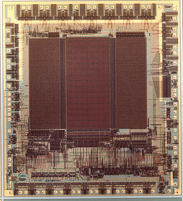
| Control | DC335 | 252x270 | 80,000 sites | The Control chip implements the microword access and sequencing functions
of the J-11 chip set. Its key features are:
Power: 0.5W |
| FPA | DC321 | 290x260 | 34,000 | The J-11 FPA is a high performance, single chip, floating point accelerator
for the J-11 chip set. Its key features are:
Power: 2.5W. |
The J-11 was introduced late in 1983 at 3.75Mhz; subsequent tweaks pushed the performance to 4.5Mhz. The FPA was introduced in 1984. The FPA was used as the basis for the MicroVAX Floating Point Unit and the V-11 F chip.
Most of DEC's limited chip design resources were focused on building a VLSI VAX (V-11). J-11 had to be built with an external partner. Based on the favorable results with Harris Semiconductor's 6120 PDP-8 microprocessor project, J-11 was set up as a co-development with Harris. DEC did the architecture and logic design, Harris the circuit design and layout.
With its ambitious speed and functional goals, geographically split team (DEC was in Maynard, Massachusetts, and Harris was in Melbourne, Florida), and primitive CAD tools, J-11 was in every sense a "chip too far". The complexity, size, and speed requirements of the chips overwhelmed Harris. The schedule slipped badly, and the Data chip grew much larger than anticipated. Due to circuit design problems, the first pass parts barely ran at 1.25Mhz. It required many passes, and many fixes, to get the chip set to function at 3.75Mhz and then 4.5Mhz. It never reached the original goal of 5Mhz. Harris had recurring problems yielding the chip, and attempts to second source the process at DEC didn't work out (DEC's CMOS processes were N-well rather than P-well).
The FPA also proved to be an ill-starred chip, with latent bugs requiring its recall from the field on two separate occasions. These problems did not show up in the derived designs for MicroVAX and V-11.
J-11 included some notable firsts. In particular, it was the first DEC design to use computer-based interconnect verification. Because the schematics were hand-drawn, an army of coops and volunteers manually created a netlist for the chip. This was then checked against the Calma layout database
J-11 was my first experience in managing a chip, and I didn't get to see the middle-game. In 1981, with design still going on, I was asked to run the Advanced Development team of the newly formed Semiconductor Engineering Group. I turned the project over to Dan Casaletto (I don't think he's forgiven me since). When I became manager of the Microprocessor Group in October, 1984, J-11 again fell into my bailiwick. It appears as a theme in the Group's monthly reports (always with problems attached) until mid1986.
Over the years, there have been numerous attempts to recast J-11 in more modern technologies, from gate arrays to FPGA's. The paper schematics, and the idiosynchratic circuit design, have defeated all efforts.
Updated 24-Feb-2008 by Bob Supnik (simh AT trailing-edge DOT com - anti-spam encoded)